- 您现在的位置:买卖IC网 > Sheet目录308 > ADUM5404CRWZ (Analog Devices Inc)IC ISOLATOR 4CH DCDC CONV 16SOIC
�� �
�
�Data� Sheet�
�Given� the� geometry� of� the� receiving� coil� in� the� ADuM5401� /�
�ADuM5402� /� ADuM5403� /� ADuM5404� ,� and� an� imposed�
�requirement� that� the� induced� voltage� be,� at� most,� 50%� of� the�
�0.5� V� margin� at� the� decoder,� a� maximum� allowable� magnetic�
�field� is� calculated� as� shown� in� Figure� 27.�
�100�
�10�
�1�
�0.1�
�0.01�
�ADuM5401/ADuM5402/ADuM5403/ADuM5404�
�Note� that,� at� combinations� of� strong� magnetic� field� and� high�
�frequency,� any� loops� formed� by� PCB� traces� can� induce� error�
�voltages� sufficiently� large� to� trigger� the� thresholds� of� succeeding�
�circuitry.� Exercise� care� in� the� layout� of� such� traces� to� avoid� this�
�possibility.�
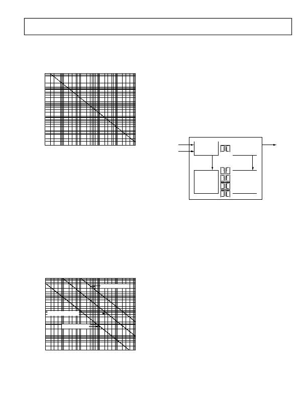
�POWER� CONSUMPTION�
�The� V� DD1� power� supply� input� provides� power� to� the� i� Coupler� data�
�channels,� as� well� as� to� the� power� converter.� For� this� reason,� the�
�quiescent� currents� drawn� by� the� data� converter� and� the� primary�
�and� secondary� input/output� channels� cannot� be� determined� sepa-�
�rately.� All� of� these� quiescent� power� demands� have� been� combined�
�into� the� I� DD1� (Q)� current,� as� shown� in� Figure� 29.� The� total� I� DD1� supply�
�current� is� the� sum� of� the� quiescent� operating� current;� the� dynamic�
�current,� I� DD1� (D)� ,� demanded� by� the� I/O� channels;� and� any� external�
�I� ISO� load.�
�I� DD1(Q)�
�I� ISO�
�0.001�
�1k�
�10k� 100k� 1M� 10M�
�MAGNETIC� FIELD� FREQUENCY� (Hz)�
�100M�
�I� DD1(D)�
�CONVERTER�
�PRIMARY�
�CONVERTER�
�SECONDARY�
�Figure� 27.� Maximum� Allowable� External� Magnetic� Flux� Density�
�For� example,� at� a� magnetic� field� frequency� of� 1� MHz,� the� maximum�
�allowable� magnetic� field� of� 0.2� kgauss� induces� a� voltage� of� 0.25� V� at�
�the� receiving� coil.� This� voltage� is� approximately� 50%� of� the� sensing�
�threshold� and� does� not� cause� a� faulty� output� transition.� Similarly,� if�
�such� an� event� occurs� during� a� transmitted� pulse� (and� is� of� the�
�worst-case� polarity),� it� reduces� the� received� pulse� from� >1.0� V� to�
�I� DDP(D)�
�PRIMARY�
�DATA�
�INPUT/OUTPUT�
�4-CHANNEL�
�I� ISO(D)�
�SECONDARY�
�DATA�
�INPUT/OUTPUT�
�4-CHANNEL�
�0.75� V,� still� well� above� the� 0.5� V� sensing� threshold� of� the� decoder.�
�The� preceding� magnetic� flux� density� values� correspond� to� specific�
�current� magnitudes� at� given� distances� from� the� ADuM5401� /�
�ADuM5402� /� ADuM5403� /� ADuM5404� transformers.� Figure� 28�
�expresses� these� allowable� current� magnitudes� as� a� function� of�
�frequency� for� selected� distances.� As� shown� in� Figure� 28,� the�
�ADuM5401� /� ADuM5402� /� ADuM5403� /� ADuM5404� are� extremely�
�immune� and� can� be� affected� only� by� extremely� large� currents�
�operated� at� high� frequency� very� close� to� the� component.� For� the�
�1� MHz� example,� a� 0.5� kA� current� placed� 5� mm� away� from� the�
�ADuM5401� /� ADuM5402� /� ADuM5403� /� ADuM5404� is� required�
�Figure� 29.� Power� Consumption� Within� the�
�ADuM5401� /� ADuM5402� /� ADuM5403� /� ADuM5404�
�Both� dynamic� input� and� output� current� is� consumed� only�
�when� operating� at� channel� speeds� higher� than� the� refresh� rate,�
�f� r� .� Each� channel� has� a� dynamic� current� determined� by� its� data�
�rate.� Figure� 21� shows� the� current� for� a� channel� in� the� forward�
�direction,� which� means� that� the� input� is� on� the� primary� side� of�
�the� part.� Figure� 22� shows� the� current� for� a� channel� in� the� reverse�
�direction,� which� means� that� the� input� is� on� the� secondary� side� of�
�the� part.� Both� figures� assume� a� typical� 15� pF� load.� The� follow-�
�ing� relationship� allows� the� total� I� DD1� current� to� be� calculated:�
�to� affect� the� operation� of� the� device.�
�I� DD1� =� (� I� ISO� ×� V� ISO� )/(� E� ×� V� DD1� )� +� Σ� I� CHn� ;� n� =� 1� to� 4�
�(1)�
�1k�
�100�
�10�
�1�
�DISTANCE = 100mm�
�DISTANCE� =� 1m�
�where:�
�I� DD1� is� the� total� supply� input� current.�
�I� CHn� is� the� current� drawn� by� a� single� channel� determined� from�
�Figure� 21� or� Figure� 22,� depending� on� channel� direction.�
�I� ISO� is� the� current� drawn� by� the� secondary� side� external� load.�
�E� is� the� power� supply� efficiency� at� 100� mA� load� from� Figure� 11�
�at� the� V� ISO� and� V� DD1� condition� of� interest.�
�DISTANCE = 5mm�
�0.1�
�0.01�
�1k�
�10k�
�100k�
�1M�
�10M�
�100M�
�MAGNETIC� FIELD� FREQUENCY� (Hz)�
�Figure� 28.� Maximum� Allowable� Current� for� Various� Current-to-�
�ADuM5401� /� ADuM5402� /� ADuM5403� /� ADuM5404� Spacings�
�Rev.� C� |� Page� 23� of� 28�
�发布紧急采购,3分钟左右您将得到回复。
相关PDF资料
ADUM6132ARWZ-RL
IC GATE DRIVER ISOLATED 16-SOIC
ADUM6201CRIZ
ISOLATED DC-DC CONV 2CH 16SOIC
ADUM6404ARWZ
IC ISOLATOR 4CH DCDC CONV 16SOIC
ADUM7241CRZ-RL7
ISOLATOR DGTL 1KVRMS 2CH 8SOIC
ADUM7440CRQZ-RL7
IC DIGITAL ISOLATOR 4CH 16QSOP
ADUM7510BRQZ
IC DGTL ISOLATOR 5CH 16QSOP
ADZS-21364-EZLITE
KIT EVAL EZ LITE ADDS-21364
ADZS-21371-EZLITE
KIT EVAL EZLITE ADZS-21371
相关代理商/技术参数
ADUM5404CRWZ1
制造商:AD 制造商全称:Analog Devices 功能描述:Quad-Channel Isolators with Integrated DC-to-DC Converter
ADUM5404CRWZ2
制造商:AD 制造商全称:Analog Devices 功能描述:Quad-Channel Isolators with Integrated DC-to-DC Converter
ADUM5404CRWZ-RL
功能描述:IC ISOLATOR 4CH DCDC CONV 16SOIC RoHS:是 类别:隔离器 >> 数字隔离器 系列:IsoPower®, iCoupler® 产品培训模块:IsoLoop® Isolator 标准包装:50 系列:IsoLoop® 输入 - 1 侧/2 侧:5/0 通道数:5 电源电压:3 V ~ 5.5 V 电压 - 隔离:2500Vrms 数据速率:110Mbps 传输延迟:12ns 输出类型:CMOS 封装/外壳:16-SOIC(0.154",3.90mm 宽) 供应商设备封装:16-SOIC N 包装:管件 工作温度:-40°C ~ 85°C 其它名称:390-1053-5
ADUM540X
制造商:AD 制造商全称:Analog Devices 功能描述:Isolated DC/DC Converter
ADUM540XWXRWZ
功能描述:DGTL ISO 2.5KV GEN PURP 16SOIC 制造商:analog devices inc. 系列:* 零件状态:上次购买时间 标准包装:1
ADUM5410BRSZ
功能描述:RS232 Digital Isolator 2500Vrms 4 Channel 150Mbps 75kV/μs CMTI 24-SSOP (0.209", 5.30mm Width) 制造商:analog devices inc. 系列:iCoupler? 包装:管件 零件状态:在售 技术:磁耦合 类型:RS232 隔离式电源:是 通道数:4 输入 - 输入侧 1/输入侧 2:4/0 通道类型:单向 电压 - 隔离:2500Vrms 共模瞬态抗扰度(最小值):75kV/μs 数据速率:150Mbps 传播延迟 tpLH / tpHL(最大值):13ns,13ns 脉宽失真(最大):3ns 上升/下降时间(典型值):2.5ns,2.5ns 电压 - 电源:1.7 V ~ 5.5 V 工作温度:-40°C ~ 105°C 封装/外壳:24-SSOP(0.209",5.30mm 宽) 供应商器件封装:24-SSOP 标准包装:59
ADUM5410BRSZ-RL7
功能描述:RS232 Digital Isolator 2500Vrms 4 Channel 150Mbps 75kV/μs CMTI 24-SSOP (0.209", 5.30mm Width) 制造商:analog devices inc. 系列:iCoupler? 包装:带卷(TR) 零件状态:在售 技术:磁耦合 类型:RS232 隔离式电源:是 通道数:4 输入 - 输入侧 1/输入侧 2:4/0 通道类型:单向 电压 - 隔离:2500Vrms 共模瞬态抗扰度(最小值):75kV/μs 数据速率:150Mbps 传播延迟 tpLH / tpHL(最大值):13ns,13ns 脉宽失真(最大):3ns 上升/下降时间(典型值):2.5ns,2.5ns 电压 - 电源:1.7 V ~ 5.5 V 工作温度:-40°C ~ 105°C 封装/外壳:24-SSOP(0.209",5.30mm 宽) 供应商器件封装:24-SSOP 标准包装:500
ADUM5411BRSZ
功能描述:RS232 Digital Isolator 2500Vrms 4 Channel 150Mbps 75kV/μs CMTI 24-SSOP (0.209", 5.30mm Width) 制造商:analog devices inc. 系列:iCoupler? 包装:管件 零件状态:在售 技术:磁耦合 类型:RS232 隔离式电源:是 通道数:4 输入 - 输入侧 1/输入侧 2:3/1 通道类型:单向 电压 - 隔离:2500Vrms 共模瞬态抗扰度(最小值):75kV/μs 数据速率:150Mbps 传播延迟 tpLH / tpHL(最大值):13ns,13ns 脉宽失真(最大):3ns 上升/下降时间(典型值):2.5ns,2.5ns 电压 - 电源:1.7 V ~ 5.5 V 工作温度:-40°C ~ 105°C 封装/外壳:24-SSOP(0.209",5.30mm 宽) 供应商器件封装:24-SSOP 标准包装:59